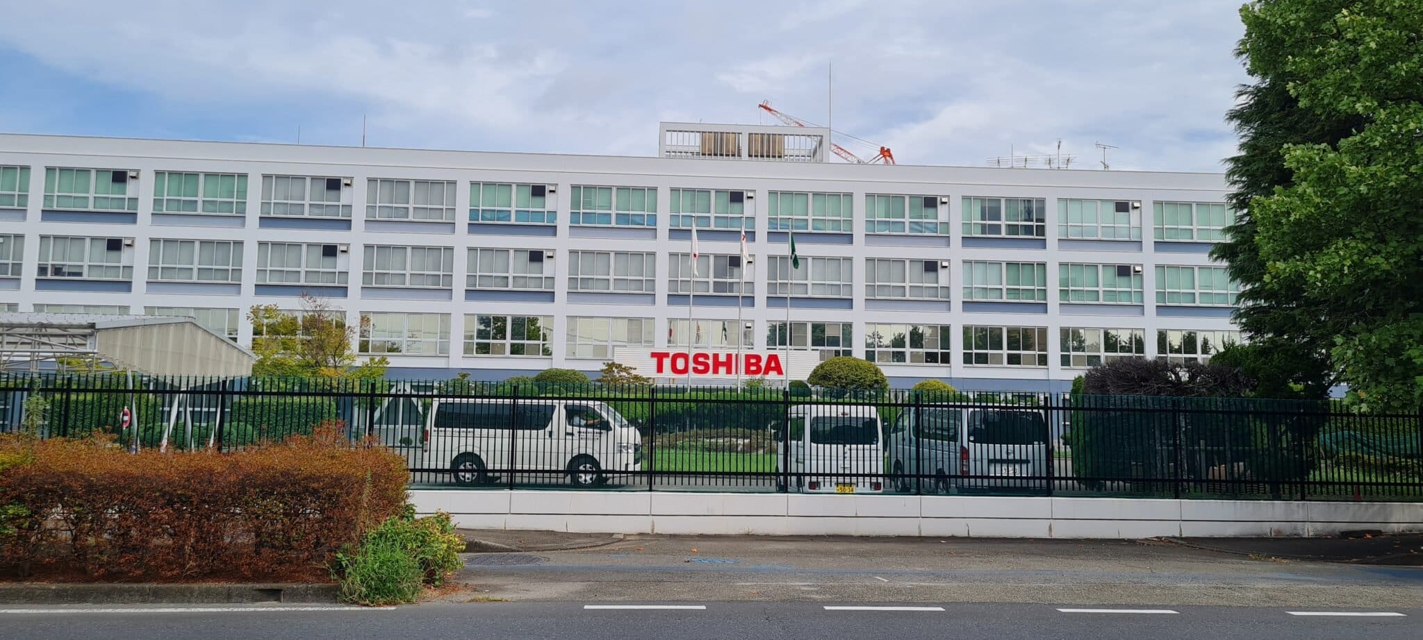
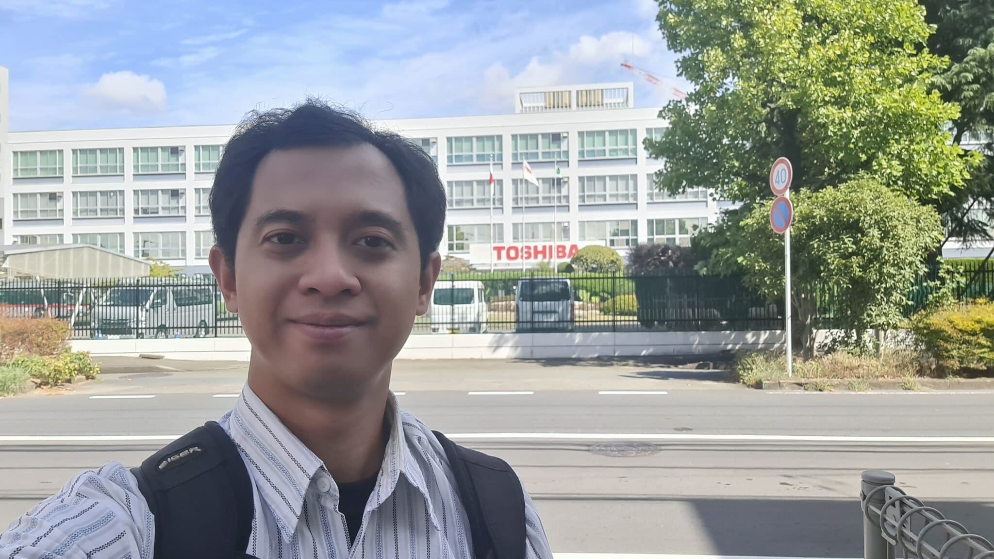
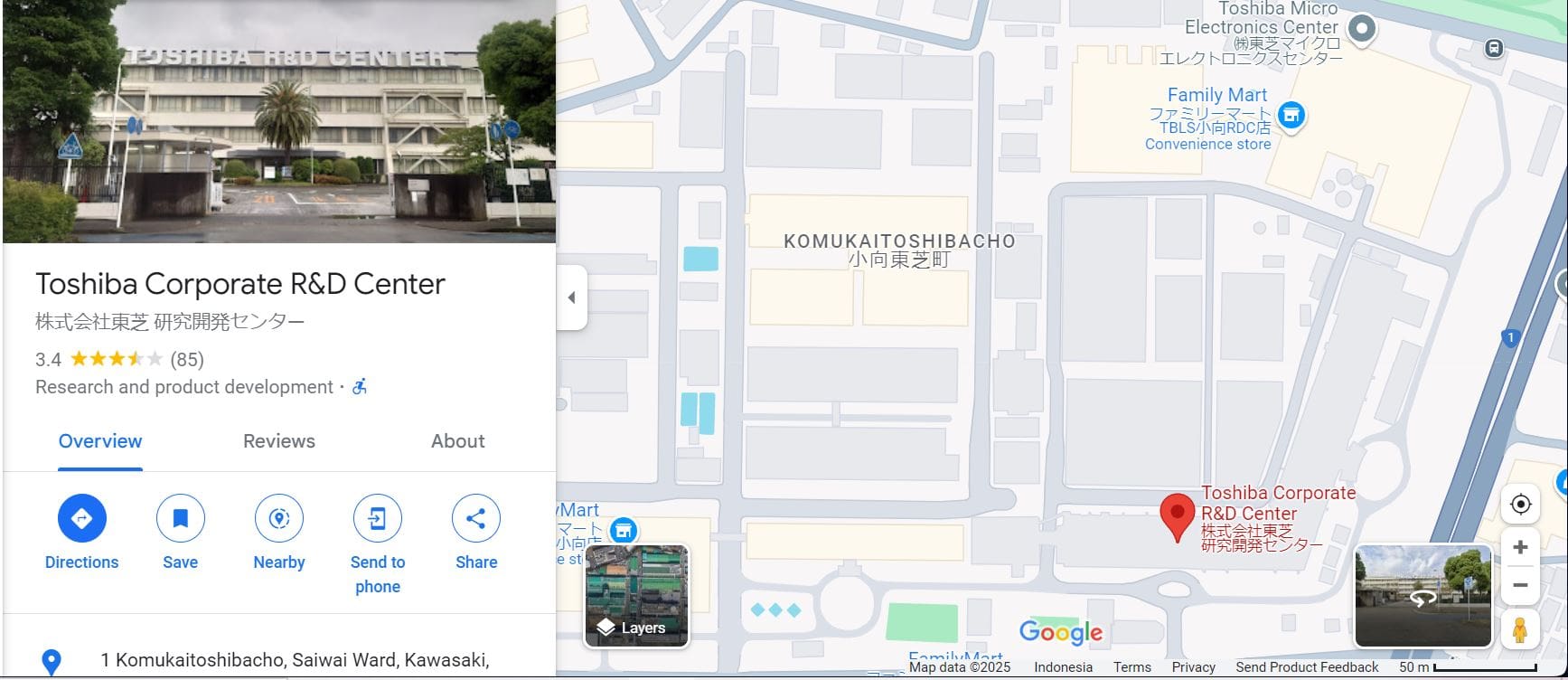
From August 28 to September 1, 2023, Dr. Sukman did an internship at Toshiba R&D Center Japan. The office location is located at the city of Kawasaki, Kanagawa Prefecture. This location is the place where Toshiba was firstly established, which was under the name of Toshiba Microcomputer Engineering Co., Ltd (https://www.toshiba.co.jp/device-sol/en/profile03.html).
The heart of Toshiba’s core technology lies on three main aspects (https://www.global.toshiba/jp/technology/corporate/rdc/recruit/fields.html):
– electronic devices
– nanomaterials
– information technologies .
For the internship, Dr. Sukman was assigned to the Advanced Device Research Laboratories, Integrated Device Technology Division. It was a truly fascinating experience, which allowed a thorough learning of the latest advancement of Toshiba’s cutting-edge technologies, especially in MEMS (microelectromechanical systems) and gas sensor devices (https://www.global.toshiba/ww/technology/corporate/rdc/rd/topics/20/2001-02.html, https://www.global.toshiba/ww/technology/corporate/rdc/rd/topics/23/2306-02.html).
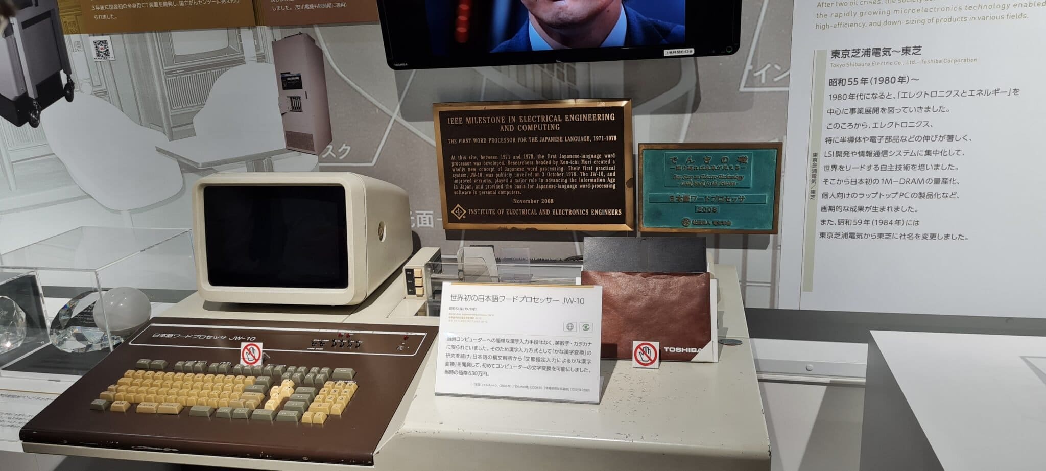
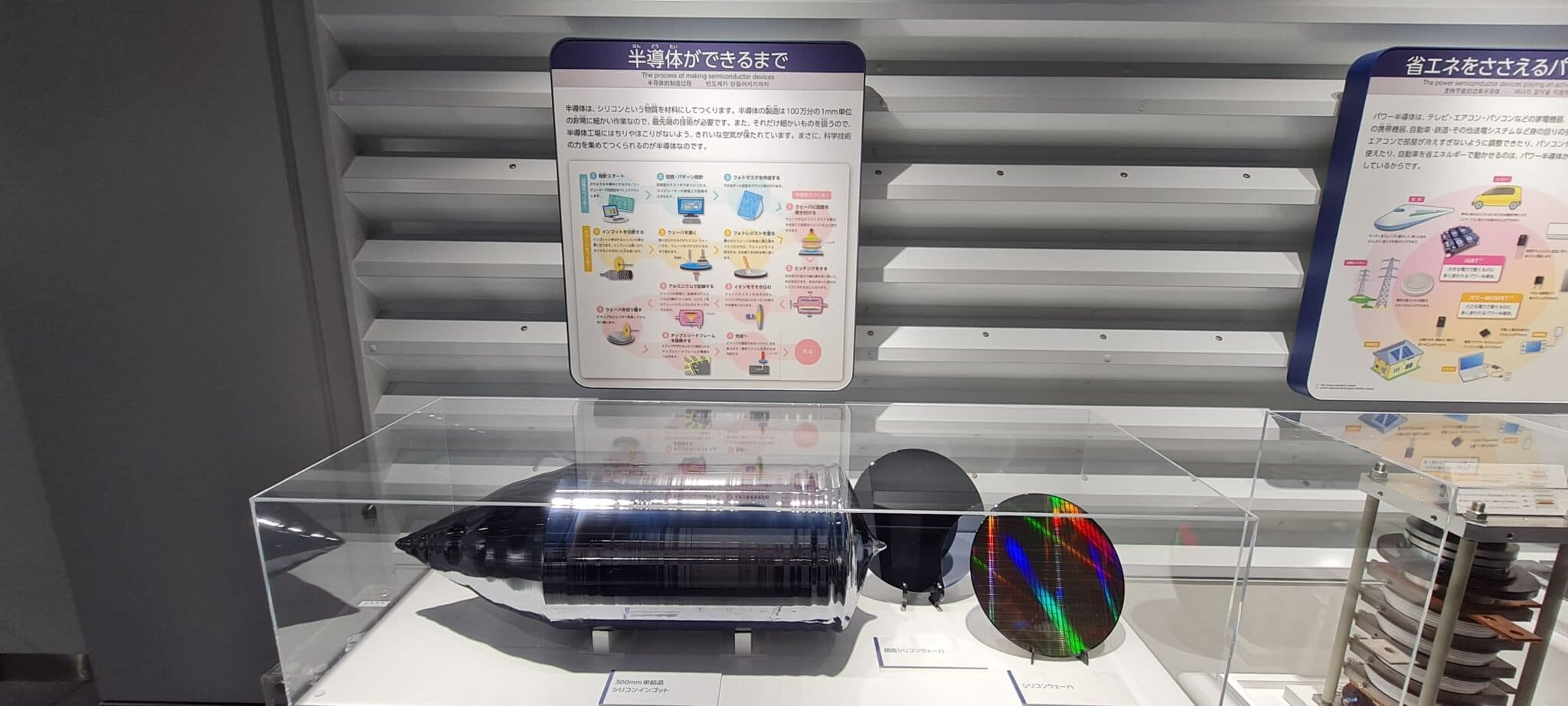
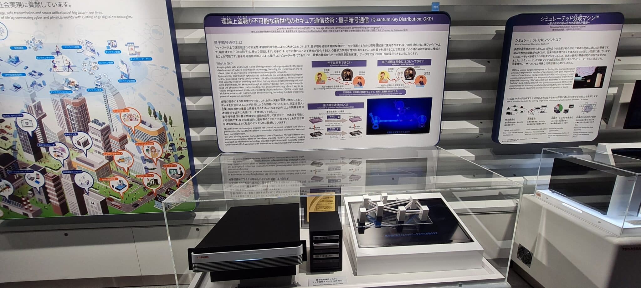
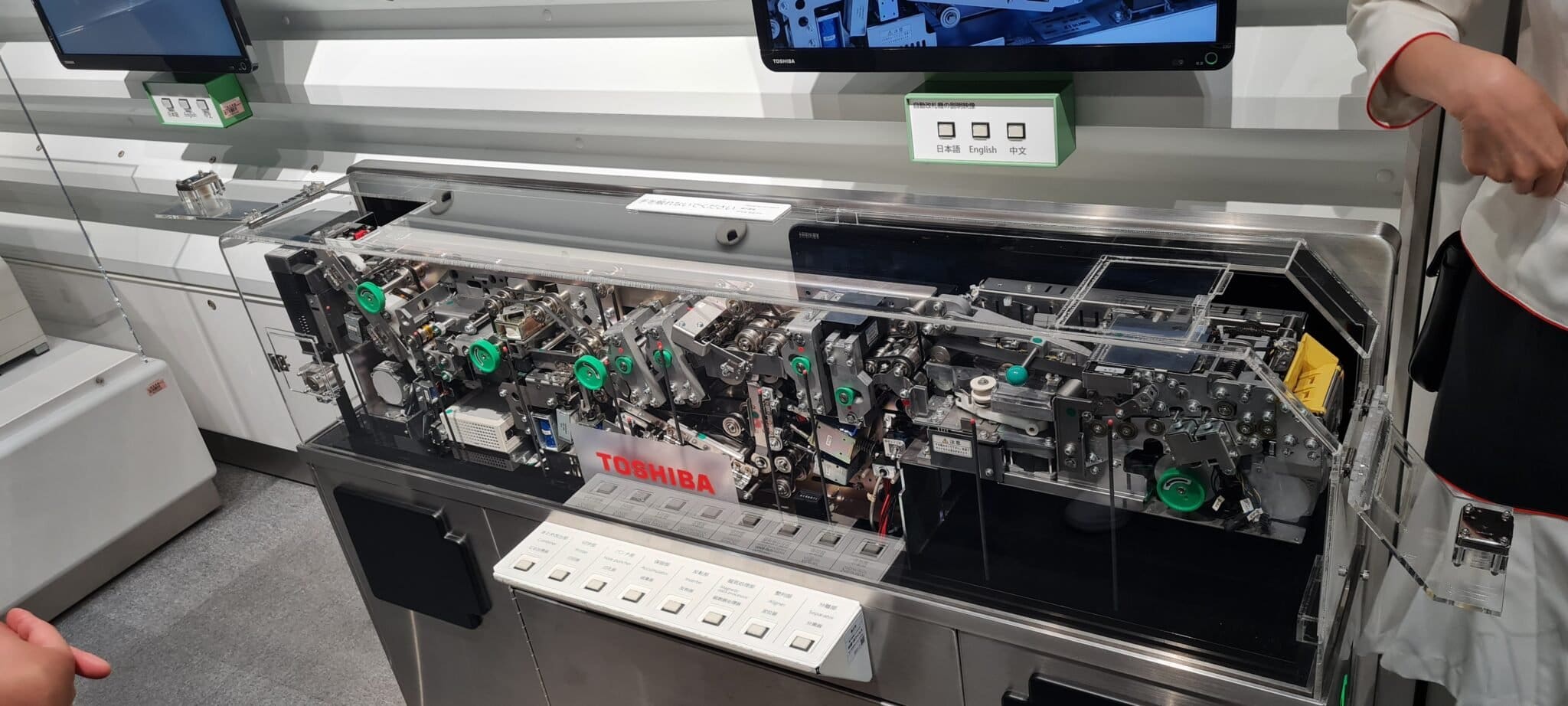
On the last day of the internship, the activities were concluded by having a visit to Toshiba Science Museum (https://maps.app.goo.gl/zZuxu1yLU3NLaLeZ6).